Author Topic: Thin Film Acquisition and Analysis in Probe for EPMA  (Read 10704 times)

Probeman

  • Emeritus
  • *****
  • Posts: 2836
  • Never sleeps...
    • John Donovan
Thin Film Acquisition and Analysis in Probe for EPMA
« on: November 11, 2013, 05:41:35 PM »
Most of our EPMA work is quantitative thin film analysis on Si substrates and there is really nothing that difficult about it, but it does help to run through the steps I think.

The biggest difference in the acquisition for thin film characterization is that one needs to acquire x-ray intensities at multiple electron beam energies for *both* the standards and unknowns.

Strictly speaking that isn't always necessary, but we find it provides the most accurate and reproducible results.  In fact, because we will utilize all the beam energies when correcting for the matrix effects and the thin film sample geometry, we can often obtain a more "robust" analysis than using only one electron beam energy. Of course the usual caveats apply, especially surface contamination, native oxide and/or hydrocarbon layers, and insulating and/or beam sensitive films.

And don't even think that you can avoid correcting for geometry- unless you are, one, operating at extremely low overvoltages, i.e., shallow probe, two, using a very, very inclined sample to the beam, or three, your sample is thick enough that your electrons do not penetrate to the substrate, i.e., your sample is not really a thin film!

Basically we will be collecting x-ray intensities for our thin film elements, the substrate elements (to help with our thickness calculations) and also any contaminate elements such as oxygen. One time when we started seeing low totals in our thin films (yes, we also get useful totals in thin film analysis), we discovered that the samples were getting contaminated with Se from a previous deposition!

But in practice this method works very well, exactly because most of the beam does penetrate to the substrate depositing most of the energy in pure Si!  Note therefore, as general a "rule of thumb", if you detect any substrate x-rays you *must* correct for a thin film geometry in your thin samples. But remember, because we are working with thin films, we are working with fewer atoms (50 nm = 500 atoms thick!), therefore you should treat thin film analyses as you would any trace element measurements with all necessary attention paid to the background characterization.

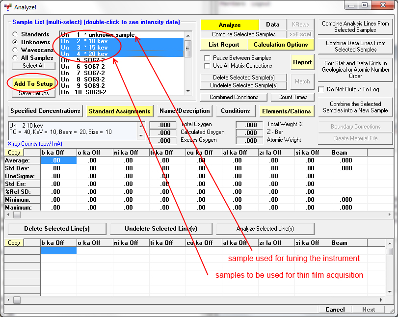
Ok, so the first step is to create a sample setup containing all the elements you need. Once you are tuned up and everything looks good (you did remember to run a careful wavescan to check for interfering off-peaks didn't you?), you will create three new sample setups based on the first and name them for the beam energies that they will have, for example 10 keV, 15 keV and 20 keV. 

Also consider using multi-point backgrounds for highly variable thin film compositions where the background positions utilized for the background correction are "dynamic" and can change "on the fly" as discussed here:

http://probesoftware.com/smf/index.php?topic=56.msg218#msg218

Of course the actual multiple voltages you utilize depends on the thickness of the thin film and the elements and x-ray lines you are using. Thinner films require lower voltages and lower energy x-ray lines sometimes. It is suggested that you model the film's likely chemistry and thickness and decide which voltages will produce the largest change in intensity with a change in electron beam energy.


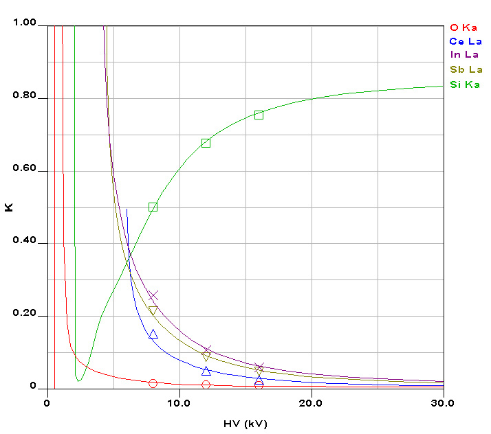
What we are after is a variation in the thin film element x-ray intensities as a function of beam energy as seen here:


The lines are the model (PAP) and the symbols are the EPMA measurements.  From these measurements we can obtain both the composition and thickness of the film. Note that the signal from the substrate increases as the beam energy is increased.

More caveats, it is very difficult to measure a thin film containing an element that is also in the substrate. In the above case oxygen is present in the film, so we would not want to try measuring a thin film for oxygen on a substrate of, for example MgO. Or say, SiGe films on Si, though it *can* be done if the thickness is already known, see this paper for more details:

http://epmalab.uoregon.edu/pdfs/Determination%20of%20Ni-Si%20Ultra-thin%20Films,%20Phung,%20et.%20al.,%202008.pdf

Next here's an example using La lines for mid-Z elements and this film is even thinner than the previous one. Also note the oxygen native oxide intensity increases as the voltage is lowered.


So now back to our acquisition.

After creating and naming our sample setups for the beam energies we decided on, we then change the operating voltage on each sample (from the Analyze! window is best because then the instrument doesn't actually have to change beam energies) using the Conditions button.

Next we want to save these samples as sample setups that can be referenced for digitizing our samples. This is easily done by selecting all three samples and clicking the Add To Setup button in the Analyze! window as seen here:


Now we are ready to digitize our unknowns (assuming the standard positions have already been loaded into the Automate! window) using the Digitize window.

I generally digitize between 6 and 10 points per thin film because they are almost perfectly uniform when deposited using thermal evaporation, but films that are deposited by laser ablation can vary in both thickness *and* composition, so be careful.  You do not want to average together points during the analysis that have different thickness and/or chemistry.

Once your points are digitized (and I usually check that I get all the little chips mounted on a 25 mm Al stub by using the StageMap window as seen here):


You can next select all your standards and unknown position samples in the Automate! window:


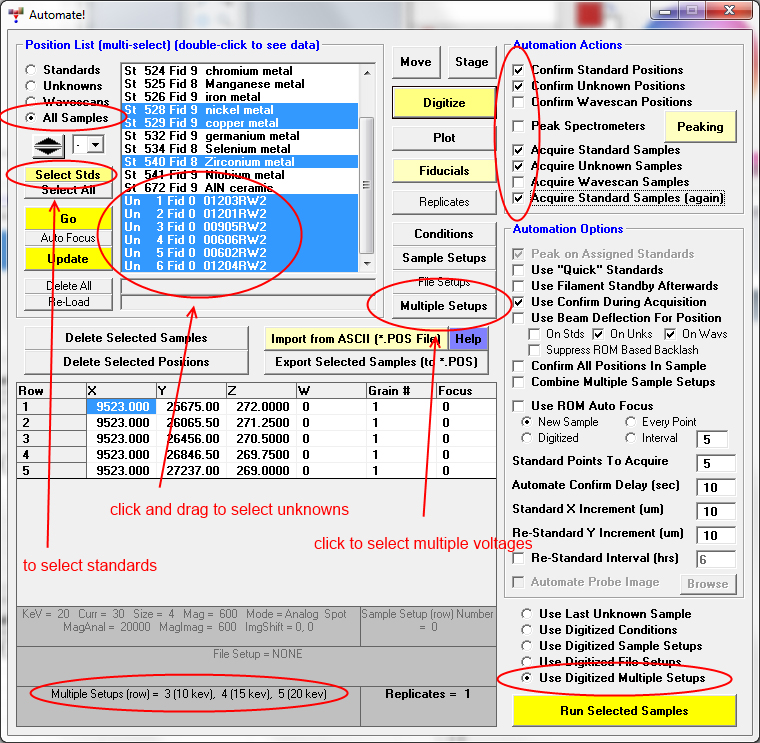
select the three sample setups for your three beam energies, and note the "automation basis" is now Use Digitized Multiple Setups.

And away you go!
« Last Edit: October 24, 2016, 11:33:08 AM by John Donovan »
The only stupid question is the one not asked!

Gareth D Hatton

  • Professor
  • ****
  • Posts: 51
Re: Thin Film Acquisition and Analysis in Probe for EPMA
« Reply #1 on: November 12, 2013, 02:01:55 AM »
Thank you for this, it is a clear guide should I ever have to do this type of analysis. ;D

Probeman

  • Emeritus
  • *****
  • Posts: 2836
  • Never sleeps...
    • John Donovan
Re: Thin Film Acquisition and Analysis in Probe for EPMA
« Reply #2 on: January 14, 2014, 12:56:27 PM »
If you want to know why multi-voltage EPMA (WDS) is the best tool for the job of characterizing the composition (and thickness) of thin films deposited on substrates, a look at the following images should suffice:


and this:


The full PPT presentation is here if you are interested:

http://epmalab.uoregon.edu/publ/Nano-2011_TEPNA.ppt
The only stupid question is the one not asked!

John Donovan

  • Administrator
  • Emeritus
  • *****
  • Posts: 3275
  • Other duties as assigned...
    • Probe Software
Re: Thin Film Acquisition and Analysis in Probe for EPMA
« Reply #3 on: June 20, 2014, 02:22:45 PM »
Usually, the measured k-ratios (at multiple beam energies), for thin film samples are then exported from Probe for EPMA and corrected for sample geometry using an external application such as STrataGEM or GMRFilm using this window accessible from the Output menu:


This is the easiest and most accurate solution for determination of thin films where both the thickness and composition are unknown, but it should be noted that for thin films that are "unsupported" or deposited on a low Z substrate (does Si qualify as "low" Z? It depends... on the physics details!) and where the film thickness (and density) are fairly well known, one can utilize a variation on the particle correction procedures in Probe for EPMA that are described here for particles:

http://probesoftware.com/smf/index.php?topic=281.0

Normally, in thin film analysis where the thickness is unknown we measure the k-ratios at multiple beam energies including the intensities emitted from the substrate (usually Si Ka and O ka for Si wafer depositions), in order to help constrain the thin film thickness during the physics interation and allow solving for composition and thickness simultaneously.

However, in the case of a known thickness we could utilize a single beam energy, although it may help estimate accuracy by utilizing several beam voltages.  And because the substrate is not included in this "particle" calculation we'll want to want an unsupported film or low Z substrate to minimize fluorescence issues and *not* measure the substrate element.  To see what I mean let's start with a roughly 50 nm Mo,W oxide thin film deposited on a Si wafer and analyze for Mo, W, O (and also Si just to see why we do not want to include the substrate emissions) as seen here without any correction for thin film geometry at a beam energy of 10 keV:

Un    6 WMo oxide-1, Results in Elemental Weight Percents
 
ELEM:       Mo       W       O      Si
BGDS:      LIN     LIN     EXP    HIGH
TIME:    60.00   60.00   60.00   60.00
BEAM:    29.94   29.94   29.94   29.94

ELEM:       Mo       W       O      Si   SUM 
   162   2.924  14.522  12.619  70.344 100.409
   163   2.902  14.240  12.310  69.995  99.447
   164   2.926  14.447  12.549  70.279 100.202
   165   2.926  14.674  12.355  70.107 100.062
   166   2.912  14.351  12.377  70.229  99.869
   167   2.911  14.180  12.349  70.226  99.666
   168   2.910  14.269  12.367  70.130  99.675
   169   2.889  14.434  12.421  70.069  99.813
   170   2.973  14.324  12.479  70.033  99.808
   171   2.846  14.386  12.244  70.265  99.742
   172   2.777  14.141  12.222  70.068  99.208
   173   2.926  14.266  12.043  70.447  99.682
   174   2.849  14.247  12.173  70.423  99.692
   175   2.911  14.408  12.391  70.307 100.017
   176   2.894  13.969  12.224  70.237  99.324

AVER:    2.898  14.324  12.342  70.210  99.774
SDEV:     .046    .169    .148    .140    .317
SERR:     .012    .044    .038    .036
%RSD:     1.57    1.18    1.20     .20
STDS:      542     574     913     514


The above analysis is a great example of "spurious accuracy" in that the seemingly good total is completely wrong.  Why? Because the Si is not in the film and including it in the matrix correction is not a physical model. We can check this because we know the film chemistry should be approximately (Mo,W)O3 or 1 to 3 cation to oxygen and the following atomic percent output is clearly not even close as seen here:

Un    6 WMo oxide-1, Results in Atomic Percents

ELEM:       Mo       W       O      Si   SUM 
   162    .896   2.321  23.179  73.604 100.000
   163    .898   2.299  22.836  73.968 100.000
   164    .898   2.314  23.098  73.690 100.000
   165    .903   2.362  22.855  73.880 100.000
   166    .897   2.308  22.869  73.926 100.000
   167    .898   2.282  22.837  73.983 100.000
   168    .898   2.298  22.883  73.922 100.000
   169    .891   2.323  22.969  73.817 100.000
   170    .916   2.303  23.059  73.722 100.000
   171    .879   2.319  22.675  74.128 100.000
   172    .860   2.286  22.704  74.150 100.000
   173    .905   2.303  22.342  74.450 100.000
   174    .880   2.296  22.540  74.285 100.000
   175    .896   2.314  22.869  73.921 100.000
   176    .895   2.254  22.664  74.187 100.000

AVER:     .894   2.305  22.825  73.975 100.000
SDEV:     .013    .024    .217    .231    .000
SERR:     .003    .006    .056    .060
%RSD:     1.45    1.03     .95     .31


The same sample but calculated at 20 keV, gives yet another set of different but also wrong values:

Un    8 WMo oxide-1, Results in Elemental Weight Percents
 
ELEM:       Mo       W       O      Si
BGDS:      LIN     LIN     EXP    HIGH
TIME:    60.00   60.00   60.00   60.00
BEAM:    29.76   29.76   29.76   29.76

ELEM:       Mo       W       O      Si   SUM 
   192   1.065   3.575  10.340  91.192 106.172
   193   1.066   3.535  10.316  91.163 106.078
   194   1.060   3.653  10.295  91.339 106.348
   195   1.082   3.625  10.158  91.253 106.117
   196   1.023   3.609  10.208  91.149 105.989
   197   1.056   3.597  10.172  91.350 106.176
   198   1.077   3.552  10.176  91.511 106.317
   199   1.070   3.571  10.182  91.333 106.157
   200   1.043   3.709  10.122  90.990 105.863
   201   1.047   3.642  10.300  91.374 106.362
   202   1.008   3.536  10.090  91.469 106.104
   203   1.040   3.607  10.006  91.031 105.683
   204   1.073   3.572  10.044  91.624 106.313
   205   1.010   3.582  10.141  91.408 106.141
   206   1.007   3.613  10.193  91.307 106.120

AVER:    1.049   3.598  10.183  91.299 106.129
SDEV:     .026    .047    .098    .174    .183
SERR:     .007    .012    .025    .045
%RSD:     2.46    1.30     .96     .19
STDS:      542     574     913     514

STKF:    .9915   .9978   .1970  1.0000
STCT:   415.35  144.62  122.91  291.32

UNKF:    .0059   .0407   .0229   .8755
UNCT:     2.46    5.90   14.26  255.06
UNBG:      .22     .48    1.26     .24

ZCOR:   1.7824   .8833  4.4546  1.0428
KRAW:    .0059   .0408   .1160   .8755
PKBG:    12.01   13.32   12.30 1078.89
INT%:     ----    ----    -.18    ----
APF:      ----    ----    .999    ----

Un    8 WMo oxide-1, Results in Atomic Percents

ELEM:       Mo       W       O      Si   SUM 
   192    .283    .496  16.471  82.751 100.000
   193    .283    .490  16.443  82.783 100.000
   194    .281    .506  16.387  82.825 100.000
   195    .288    .504  16.217  82.992 100.000
   196    .272    .502  16.302  82.924 100.000
   197    .281    .499  16.223  82.997 100.000
   198    .286    .492  16.205  83.017 100.000
   199    .285    .496  16.239  82.980 100.000
   200    .278    .517  16.207  82.998 100.000
   201    .278    .504  16.389  82.829 100.000
   202    .268    .491  16.099  83.142 100.000
   203    .278    .503  16.048  83.171 100.000
   204    .285    .496  16.012  83.208 100.000
   205    .269    .497  16.175  83.059 100.000
   206    .268    .502  16.259  82.972 100.000

AVER:     .279    .500  16.245  82.976 100.000
SDEV:     .007    .007    .136    .137    .000
SERR:     .002    .002    .035    .035
%RSD:     2.41    1.38     .84     .17


Clearly still not close to 3:1, so let's "disable quant" on the Si Ka intensities and recalculate (again still without the thin film correction) and see if that improves things at all using the 10 keV intensities:

Un    6 WMo oxide-1, Results in Elemental Weight Percents
 
ELEM:       Mo       W       O      Si
BGDS:      LIN     LIN     EXP    HIGH
TIME:    60.00   60.00   60.00     ---
BEAM:    29.94   29.94   29.94     ---

ELEM:       Mo       W       O    Si-D   SUM 
   162   2.620  13.956  11.196     ---  27.772
   163   2.598  13.679  10.929     ---  27.207
   164   2.621  13.883  11.137     ---  27.641
   165   2.621  14.080  10.992     ---  27.693
   166   2.608  13.784  10.989     ---  27.382
   167   2.606  13.626  10.958     ---  27.190
   168   2.605  13.709  10.978     ---  27.292
   169   2.588  13.864  11.025     ---  27.477
   170   2.663  13.767  11.084     ---  27.514
   171   2.549  13.808  10.870     ---  27.227
   172   2.487  13.581  10.826     ---  26.895
   173   2.618  13.687  10.717     ---  27.022
   174   2.550  13.675  10.805     ---  27.031
   175   2.607  13.837  11.003     ---  27.447
   176   2.590  13.425  10.842     ---  26.857

AVER:    2.595  13.757  10.957     ---  27.310
SDEV:     .041    .160    .129     ---    .285
SERR:     .011    .041    .033     ---
%RSD:     1.58    1.16    1.18     ---
STDS:      542     574     913     ---

STKF:    .9901   .9971   .3323     ---
STCT:   162.36   73.01  135.61     ---

UNKF:    .0206   .1188   .0605     ---
UNCT:     3.37    8.70   24.70     ---
UNBG:      .18     .25    1.48     ---

ZCOR:   1.2613  1.1580  1.8102     ---
KRAW:    .0208   .1192   .1821     ---
PKBG:    19.91   36.16   17.74     ---
INT%:     ----    ----    -.60     ---
APF:      ----    ----    .980     ---

Un    6 WMo oxide-1, Results in Atomic Percents

ELEM:       Mo       W       O    Si-D   SUM 
   162   3.401   9.453  87.146     --- 100.000
   163   3.452   9.484  87.064     --- 100.000
   164   3.420   9.452  87.128     --- 100.000
   165   3.455   9.683  86.862     --- 100.000
   166   3.445   9.503  87.052     --- 100.000
   167   3.455   9.427  87.118     --- 100.000
   168   3.447   9.465  87.088     --- 100.000
   169   3.408   9.527  87.064     --- 100.000
   170   3.489   9.414  87.097     --- 100.000
   171   3.401   9.616  86.983     --- 100.000
   172   3.339   9.514  87.147     --- 100.000
   173   3.537   9.649  86.814     --- 100.000
   174   3.424   9.582  86.994     --- 100.000
   175   3.439   9.525  87.036     --- 100.000
   176   3.471   9.390  87.139     --- 100.000

AVER:    3.439   9.512  87.049     --- 100.000
SDEV:     .045    .087    .100     ---    .000
SERR:     .012    .022    .026     ---
%RSD:     1.31     .91     .11     ---


The total is very low because we have not yet turned on the thin film correction, and the cation to oxide ratios are better than before, but still not 1:3. So now let's turn on the thin film correction as seen here:


where I have selected the "Thin Film" option, entered 50 nm for the thickness (0.05 um) and 5 for the density (I have no idea what it might actually be from a spin cast deposition subsequently baked)...

and output the compositions for all three beam energies, first at 10 keV:

Un    6 WMo oxide-1, Results in Atomic Percents

ELEM:       Mo       W       O    Si-D   SUM 
   162   4.497  14.884  80.619     --- 100.000
   163   4.570  14.949  80.481     --- 100.000
   164   4.524  14.887  80.589     --- 100.000
   165   4.574  15.296  80.130     --- 100.000
   166   4.560  14.980  80.459     --- 100.000
   167   4.574  14.853  80.574     --- 100.000
   168   4.563  14.915  80.522     --- 100.000
   169   4.508  15.014  80.477     --- 100.000
   170   4.622  14.838  80.540     --- 100.000
   171   4.499  15.165  80.336     --- 100.000
   172   4.410  14.974  80.616     --- 100.000
   173   4.690  15.256  80.054     --- 100.000
   174   4.531  15.112  80.357     --- 100.000
   175   4.551  15.018  80.431     --- 100.000
   176   4.596  14.791  80.613     --- 100.000

AVER:    4.551  14.996  80.453     --- 100.000
SDEV:     .064    .152    .172     ---    .000
SERR:     .016    .039    .044     ---
%RSD:     1.40    1.01     .21     ---


and at 15 keV:

Un    7 WMo oxide-1, Results in Atomic Percents

ELEM:       Mo       W       O    Si-D   SUM 
   177   4.512  14.040  81.448     --- 100.000
   178   4.390  14.299  81.311     --- 100.000
   179   4.513  14.393  81.094     --- 100.000
   180   4.310  14.576  81.114     --- 100.000
   181   4.533  14.327  81.141     --- 100.000
   182   4.444  14.485  81.071     --- 100.000
   183   4.507  14.191  81.302     --- 100.000
   184   4.479  14.533  80.988     --- 100.000
   185   4.401  14.717  80.882     --- 100.000
   186   4.426  14.360  81.214     --- 100.000
   187   4.504  14.552  80.944     --- 100.000
   188   4.509  14.381  81.111     --- 100.000
   189   4.504  14.566  80.931     --- 100.000
   190   4.521  14.455  81.025     --- 100.000
   191   4.526  14.298  81.176     --- 100.000

AVER:    4.472  14.411  81.117     --- 100.000
SDEV:     .064    .171    .156     ---    .000
SERR:     .017    .044    .040     ---
%RSD:     1.44    1.19     .19     ---


and finally at 20 keV:

Un    8 WMo oxide-1, Results in Atomic Percents

ELEM:       Mo       W       O    Si-D   SUM 
   192   4.379  13.480  82.141     --- 100.000
   193   4.396  13.376  82.228     --- 100.000
   194   4.362  13.794  81.844     --- 100.000
   195   4.502  13.856  81.642     --- 100.000
   196   4.253  13.773  81.974     --- 100.000
   197   4.401  13.762  81.837     --- 100.000
   198   4.491  13.598  81.911     --- 100.000
   199   4.458  13.655  81.887     --- 100.000
   200   4.347  14.198  81.455     --- 100.000
   201   4.310  13.760  81.930     --- 100.000
   202   4.246  13.690  82.063     --- 100.000
   203   4.392  14.006  81.602     --- 100.000
   204   4.520  13.830  81.650     --- 100.000
   205   4.231  13.780  81.989     --- 100.000
   206   4.195  13.817  81.988     --- 100.000

AVER:    4.365  13.758  81.876     --- 100.000
SDEV:     .103    .196    .212     ---    .000
SERR:     .027    .051    .055     ---
%RSD:     2.35    1.43     .26     ---


and we can see that the atomic rations for Mo + W to O is roughly 1:4 for all three beam energies which gives us some confidence that we might be doing something right after all!

But why is our cation to oxygen ratio still too high?  It really ought to be 1:3, not 1:4. Where could that extra oxygen be coming from? 

Well one obvious explanation is that the Si substrate is backscattering and/or fluorescing oxygen in the film from the substrate to some small but significant degree (which is why we really should be using carbon planchet substrate or a physics model such as STrataGEM or GMRFilm which includes the substrate effects)... remember, our oxide film is only some 50 nm thick and it wouldn't take much to produce some significant additional oxygen from backscatter electrons or fluorescence from the substrate.

The other obvious question is: is this substrate really oxygen free?  We know that Si wafers continue to grow their native oxide layer over time and when I asked the student: "did you etch the Si wafer prior to deposition?", the answer was, sadly, no...

Consider a 50 nm film on top of a 5 nm or so thick native oxide layer. That is an additional 10% oxygen!

So all in all a pretty good result considering that we shouldn't really be doing it this way at all.  If anyone else has measurements on a better specimen please feel free to post your examples.
John J. Donovan, Pres. 
(541) 343-3400

"Not Absolutely Certain, Yet Reliable"

John Donovan

  • Administrator
  • Emeritus
  • *****
  • Posts: 3275
  • Other duties as assigned...
    • Probe Software
Re: Thin Film Acquisition and Analysis in Probe for EPMA
« Reply #4 on: June 21, 2014, 10:20:52 AM »
Another way to evaluate the "crude but sometimes effective" thin film correction in PFE is to directly compare its results to a full treatment with multi-voltage analysis (MVA).

Here are the results of a BiSnTi thin film sample on Si calculated with STrataGEM using intensities measured at 7, 11 and 15 keV:


Note the normalized weight fractions in the column labeled "Weight". Now compare those to the results using the PFE thin film correction at the three voltages. First at 7 keV:

Un   35 alloy_1b, Results in Normalized Elemental Weight Percents (Particle Corrections)

ELEM:     Si-D       O      Se      Ti      Bi      Sn   SUM 
   241     ---    .538  57.815  10.546  23.942   7.159 100.000
   242     ---    .560  58.251  10.426  23.688   7.074 100.000
   243     ---    .544  57.984  10.434  24.106   6.932 100.000
   244     ---    .475  58.481  10.797  23.157   7.090 100.000
   245     ---    .506  58.343  10.600  23.516   7.035 100.000

AVER:      ---    .525  58.175  10.561  23.682   7.058 100.000
SDEV:      ---    .034    .271    .151    .371    .083    .000
SERR:      ---    .015    .121    .068    .166    .037
%RSD:      ---    6.49     .47    1.43    1.57    1.18

Now at 11 keV:

Un   36 alloy_1b, Results in Normalized Elemental Weight Percents (Particle Corrections)

ELEM:     Si-D       O      Se      Ti      Bi      Sn   SUM 
   246     ---    .746  59.812   9.263  23.488   6.692 100.000
   247     ---    .691  60.084   9.475  23.068   6.683 100.000
   248     ---    .671  59.548   9.356  23.792   6.633 100.000
   249     ---    .741  60.326   9.351  22.803   6.779 100.000
   250     ---    .778  60.217   9.501  22.343   7.160 100.000

AVER:      ---    .725  59.997   9.389  23.099   6.789 100.000
SDEV:      ---    .044    .316    .098    .568    .214    .000
SERR:      ---    .020    .141    .044    .254    .096
%RSD:      ---    6.04     .53    1.05    2.46    3.15

Finally at 15 keV:

Un   37 alloy_1b, Results in Normalized Elemental Weight Percents (Particle Corrections)

ELEM:     Si-D       O      Se      Ti      Bi      Sn   SUM 
   251     ---    .943  60.638   9.221  22.722   6.477 100.000
   252     ---    .657  60.977   9.153  22.544   6.669 100.000
   253     ---    .990  60.789   9.139  22.432   6.650 100.000
   254     ---    .704  60.493   9.246  22.786   6.771 100.000
   255     ---    .926  60.824   9.135  22.427   6.688 100.000

AVER:      ---    .844  60.744   9.179  22.582   6.651 100.000
SDEV:      ---    .152    .185    .051    .165    .108    .000
SERR:      ---    .068    .083    .023    .074    .048
%RSD:      ---   18.02     .30     .56     .73    1.62


As you can see even the crude "unsupported thin film" model compares well to the full substrate MVA physics model- at least in this one example!
John J. Donovan, Pres. 
(541) 343-3400

"Not Absolutely Certain, Yet Reliable"

John Donovan

  • Administrator
  • Emeritus
  • *****
  • Posts: 3275
  • Other duties as assigned...
    • Probe Software
Re: Thin Film Acquisition and Analysis in Probe for EPMA
« Reply #5 on: December 05, 2014, 10:14:15 AM »
The most recent versions of StrataGEM now require a $End statement at the end of the import file created by Probe for EPMA. And no, this change made by JF Thiot is *not* backward compatible with earlier versions of StrataGEM (don't ask me why!).

Anyway, here is the updated documentation in the Probe for EPMA help file. Basically you need to add this new keyword to the [software] section of your Probewin.ini file if you are using StrataGEM v. 5 or earlier (and maybe even some early releases of version 6 as well according to JF Thiot!).

StrataGEMVersion=6
This flag is used to add a “$End” statement at the end of the StrataGEM import file. Beginning with version 6 of StrataGEM a $End statement is required at the end of the import file.
 
However, versions of StrataGEM prior to version 6 *cannot* have a $End statement at the end of the StrataGEM import file according to JF Thiot. Whatever happened to backward compatibility?
 
Anyway, the default StrataGEM version is 6, so Probe for EPMA will add a $End statement to the end of the import file automatically, unless the StrataGEMVersion keyword in the Probewin.ini file [software] section is set to 4 or 5. Which means that users with older versions of StrataGEM will have to edit their Probewin.ini files manually.
« Last Edit: December 05, 2014, 01:53:49 PM by John Donovan »
John J. Donovan, Pres. 
(541) 343-3400

"Not Absolutely Certain, Yet Reliable"

smatveev

  • Post Doc
  • ***
  • Posts: 16
Re: Thin Film Acquisition and Analysis in Probe for EPMA
« Reply #6 on: July 17, 2015, 01:49:48 AM »
Dear John,
recently I started to work with thin electron-transparent samples prepared using FIB SEM. Such samples are mounted on copper grid, no substrate used. It can see  some potential in such analysis, particularly for high spatial resolution applications at "normal" and high voltages. Quantitative WDS of thin films is less involved compared to the bulk, but is tricky as calibration and correction philosophies have to be modified. While working on wedged samples I could observe how ZAF-based corrections stop working with sample thickness reduction. Surprisingly thin film corrections are not working properly either as absorption coefficients are rather high. I am thinking of using  Cliff - Lorimer approach and wonder what is your take on it. Would you recommend to use calibration curve routines?
Cheers,
Sergei

Probeman

  • Emeritus
  • *****
  • Posts: 2836
  • Never sleeps...
    • John Donovan
Re: Thin Film Acquisition and Analysis in Probe for EPMA
« Reply #7 on: July 17, 2015, 08:14:11 AM »
Dear John,
recently I started to work with thin electron-transparent samples prepared using FIB SEM. Such samples are mounted on copper grid, no substrate used. It can see  some potential in such analysis, particularly for high spatial resolution applications at "normal" and high voltages. Quantitative WDS of thin films is less involved compared to the bulk, but is tricky as calibration and correction philosophies have to be modified. While working on wedged samples I could observe how ZAF-based corrections stop working with sample thickness reduction. Surprisingly thin film corrections are not working properly either as absorption coefficients are rather high. I am thinking of using  Cliff - Lorimer approach and wonder what is your take on it. Would you recommend to use calibration curve routines?
Cheers,
Sergei

Hi Sergei,
With thin film samples (substrate or no substrate) one must correct for the fact that the electrons do not come to rest in the material of interest (relative to a standard).  I have found that the thin film correction in CalcZAF gives excellent results especially when the substrate is missing (TEM mounts) or is a low Z substrate where the substrate element(s) does not fluoresce any thin film elements.  Otherwise I use STRATAGem* routinely. About 60% of the work in our lab is thin films on substrates.

This post describes correcting for small particle geometries in CalcZAF, but if you use the first option (thin film without substrate), you should get good results:

http://probesoftware.com/smf/index.php?topic=281.msg2735#msg2735

* © Copyright 1993-2016 SAMx
« Last Edit: February 06, 2016, 08:08:46 AM by John Donovan »
The only stupid question is the one not asked!