Keeping in mind that I’m learning as I go…
Output from the WDS preamplifier typically is next passed to a shaping amplifier. The purpose of the shaping amplifier is to amplify the signal from the leading edge of a pulse while attenuating pulse tails and electronic noise (see figure below). A shaping amplifier constructed with multiple stages of integration after initial differentiation produces “quasi-Gaussian” pulses – in terms of
V(
t) – with large signal-to-noise ratio and narrow widths (with FWHM generally ranging between 100 ns and 20 μs). The circuit, which constitutes a band-pass filter, could be constructed simply with passive components (resistors and capacitors), but, on a plot of gain versus frequency, steeper gain “roll-off” above the passband is obtained from cascaded active filters constructed with op amps. In the two commercial designs that I’ve seen so far, initial passive C-R differentiation, constituting a high-pass filter, is followed by two cascaded active second-order low-pass filters, producing four stages of integration (“poles” in the frequency response). The Bessel filter response appears to be the most appropriate for pulse processing, as it shows better stability during transient events than the Butterworth or Chebyshev responses. A drawback of the Bessel response is that, when viewing a plot of gain versus frequency, it attenuates the signal above the “corner frequency” less steeply than the Butterworth and especially the Chebyshev response. Another drawback of the Bessel response is that gain within the passband is not as uniform as that of the second-order Butterworth response. Cremat uses the Sallen-Key topology for their CR-200 shaping amplifier, but they do not specify the filter response (see attached CR-200 application guide). In a design that I’ll address in more detail below, the multiple feedback (MFB) filter topology is used in conjunction with the Bessel response.
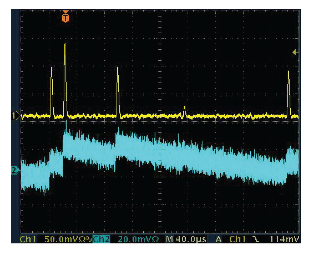
Below is a figure that shows output from the Cremat CR-110 preamplifier (bottom) as well as simultaneous filtered output from the CR-200 shaping amplifier. The shaping amplifier (with 1 μs shaping time or FWHM = 2.4 μs) dramatically reduces pulse width and equally impressively increases signal/noise:
Ideally (see below), the width of the peak produced by the shaping amplifier is controlled by the initial passive differentiation stage, with “shaping time” given as
Cin *
Rin; FWHM is obtained by multiplying by 2.4, ideally. Shaping times typically range between tens ns and 10 μs, with longer times giving better signal-to-noise ratio. A pulse from a solid-state detector would typically require a longer shaping time than one from a proportional counter because the amplitude of its signal is roughly an order of magnitude smaller than the ~3 mV signal produced by a proportional counter. Since the rise time of the pulse from the preamplifier is small, only some portion of the leading edge of the pulse (as modified by the preamplifier coupling capacitor and noise) will be characterized by d
V/d
t of appropriate magnitude to place it within the passband of the filter. Note that, in the figure above, only regions of steep d
V/d
t are amplified, with amplitude of the resulting pulse proportional to Δ
V above the surrounding low d
V/d
t + noise region (commonly consisting of superimposed pulse tails). For shorter shaping times, the passband is moved to higher frequency (greater d
V/d
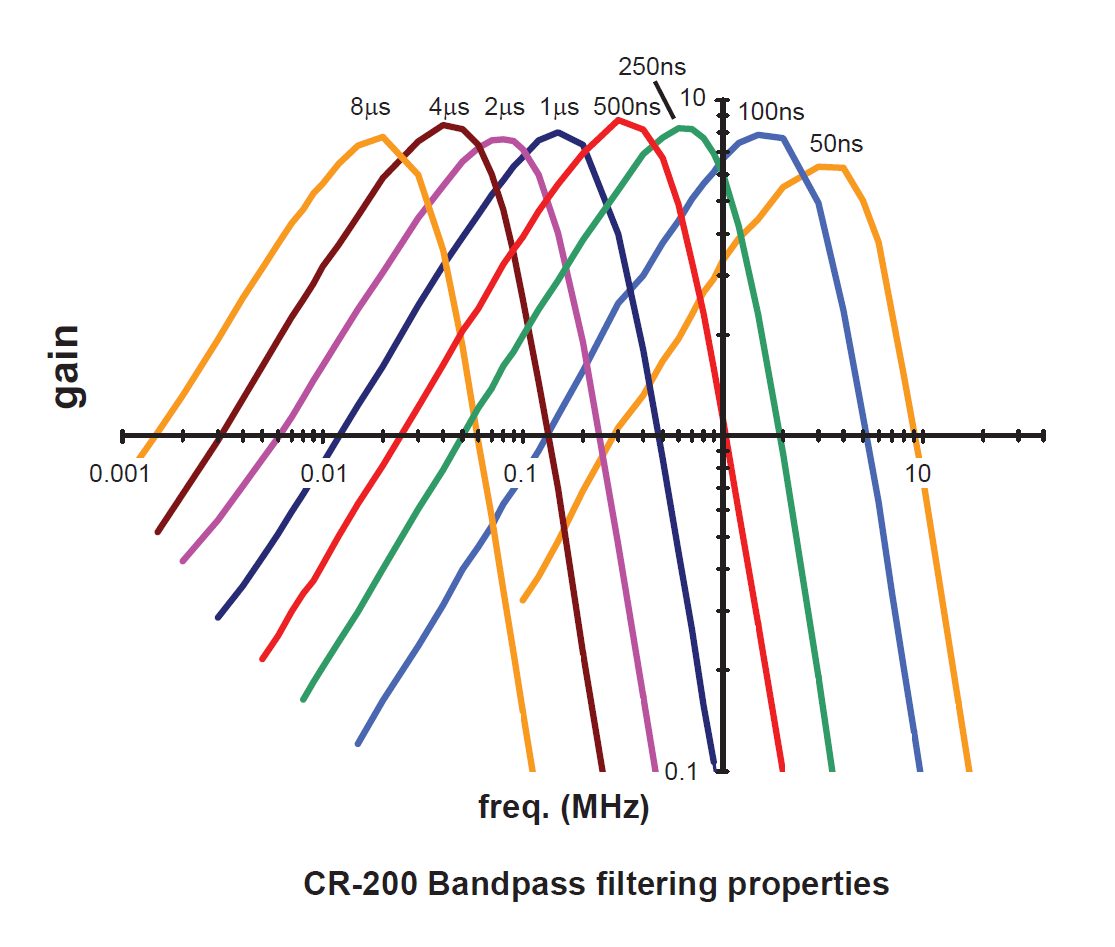
t for this case), The figure below from Cremat shows gain/attenuation as a function of frequency for the CR-200 (application guide attached) for various shaping times.
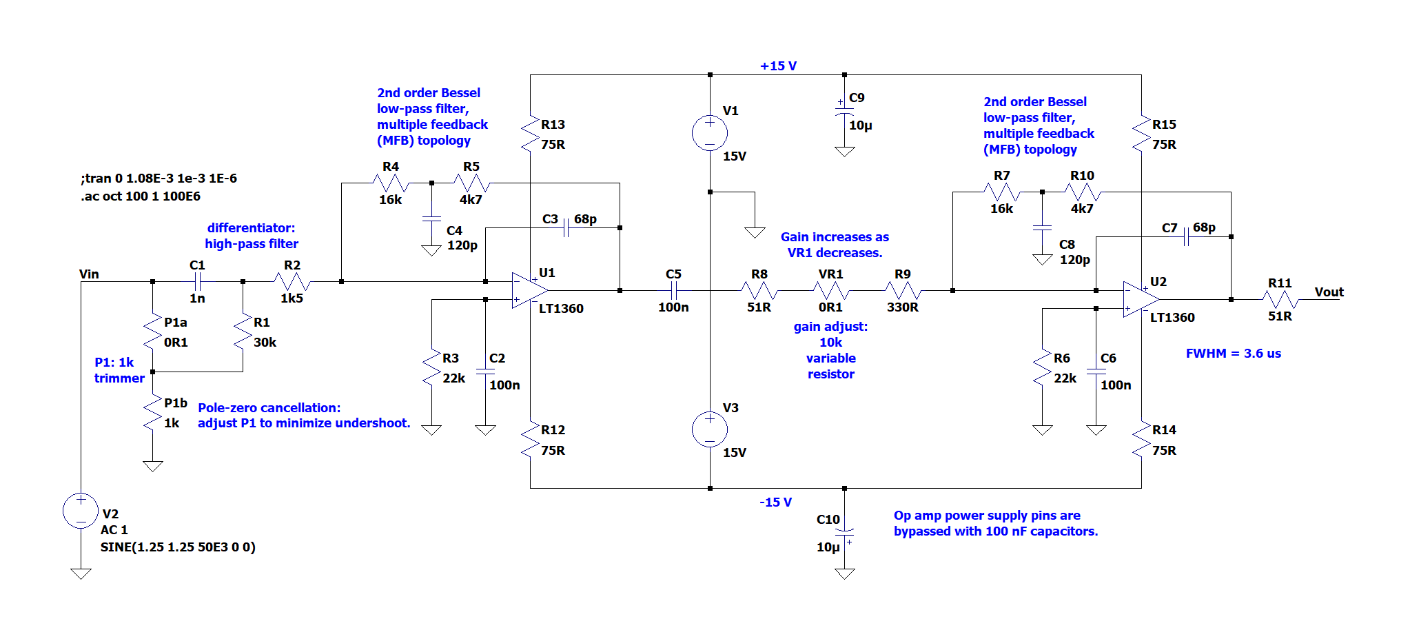
I’ve attached a paper by Perevertaylo et al. in which schematics are presented for a commercial shaping amplifier and charge-sensitive preamplifier. I’ve simulated the shaping amplifier in the
LTSpice simulator. It comprises a passive C-R differentiator followed by two cascaded second order low-pass Bessel filters constructed using the “multiple feedback” (MFB) topology. The circuit includes adjustable “pole-zero cancellation” used to compensate for undershoot on the trailing edge of the shaped pulse. The small-signal voltage gain is also adjustable by means of a variable resistor. The output pulse FWHM is stated as 4 μs. Here is the schematic (attached as a .asc file for
LTSpice):
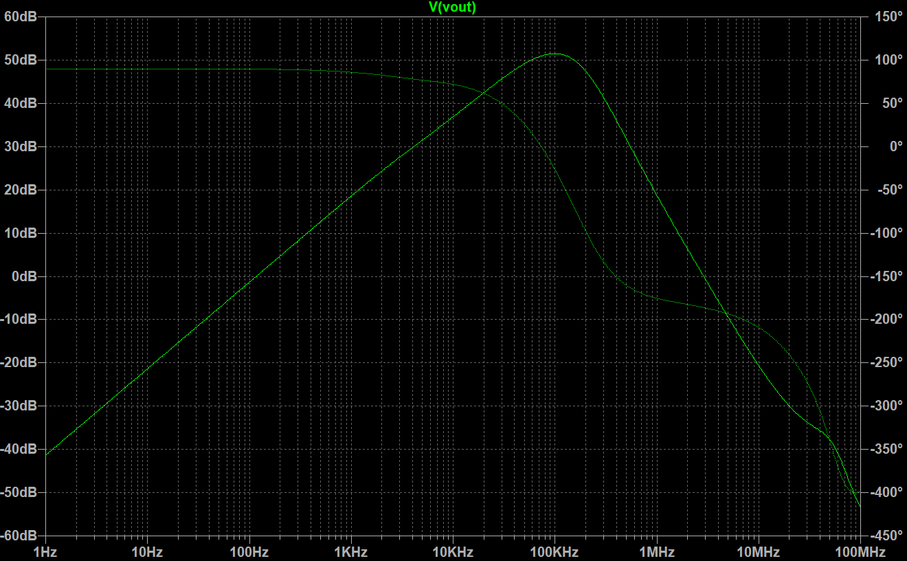
The figure below is a so-called Bode plot that shows both gain (heavier curve) and phase shift of the Perevertaylo et al. filter as a function of frequency. The passive differentiator (high-pass filter) is responsible for the 20 dB per decade slope of the gain curve at frequency below the passband. (Voltage gain [dB] = 20 × log
10 [output voltage / input voltage], i.e., 20 dB corresponds to a voltage gain of ten.) The passband is centered at about 100 kHz, which is roughly consistent with placement of the passband in the CR-200 (for interpolated shaping time = 1.5 μs). At frequencies above the passband, the active low-pass filter attenuates the signal at -40 dB per decade. According to Perevertaylo et al., gain should range between 10 and 140 (20-43 dB), while I get values between about 14 and 400 (23-52 dB); I’m not sure of the reason for the discrepancy.
Combining the JEOL preamplifier and Perevertaylo et al. shaping amplifier produces the following circuit (attached as .asc file):
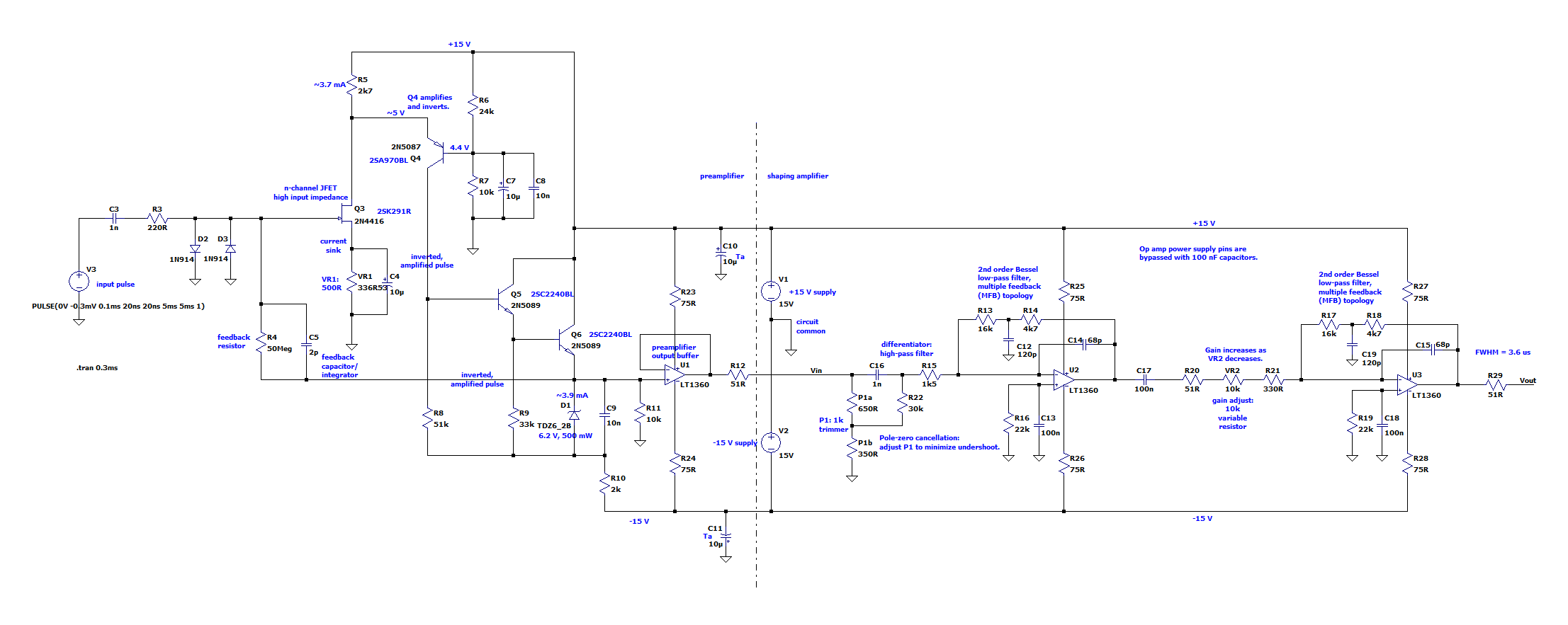
As before, when simulating the circuit in
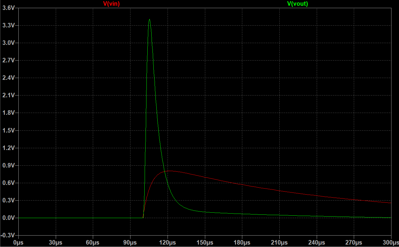
LTSpice, I’ve simply used the leading edge of a square wave as input to the preamplifier; I’ve set its amplitude at -300 μV. The preamplifier coupling capacitor, C3, can produce substantial effects on performance of the shaping amplifier, and I’ve used the simulator to assess variation in pulse width and distortion (mostly just visually) as a function of the value of C3. (The value of C3 can be viewed as a sum of C3 itself and detector and cable capacitances, which should be much smaller.) For instance, in their preamplifier, Perevertaylo et al. use a 200 pF coupling capacitor in conjunction with a (Cd,Zn)Te (CZT) detector (with 5 pF capacitance). In the femtojoule detection demonstration, Cremat uses a 10 nF coupling capacitor with a PIN photodiode (though its capacitance is only a few tens pF). The JEOL WDS preamplifier contains a 2.2 nF coupling capacitor and CAMECA, 10 nF(?). If I use a 1 nF coupling capacitor, then I get the results below. The broad, low pulse is the input signal from the preamplifier, while the tall, narrow pulse is the output from the shaping amplifier (at minimum shaping amplifier gain).
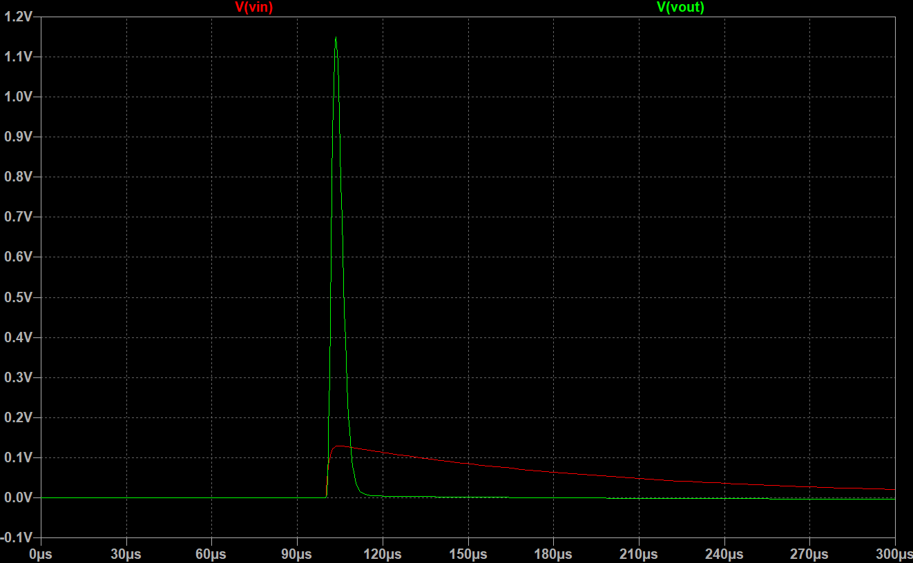
For the shaping amplifier output shown above, FWHM is about 4.3 μs, with some asymmetry in the shaped pulse apparent. The output of the shaping amplifier appears to be centered on the uppermost part of the trailing edge of the preamplifier tail pulse, but this is misleading, as formation of the shaped pulse can require a few microseconds. This becomes much clearer when the value of C3 is lowered to 100 pF (shown below). Along the tail of the input pulse, the value of d
V/d
t is too low for it to fall within the filter passband, and so the centroid of the shaped pulse must represent some portion of the leading edge of the input pulse and is delayed ~2.7 μs (at least at the centroid).
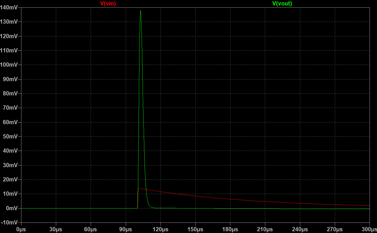
Here is a view with the time axis stretched out a little:
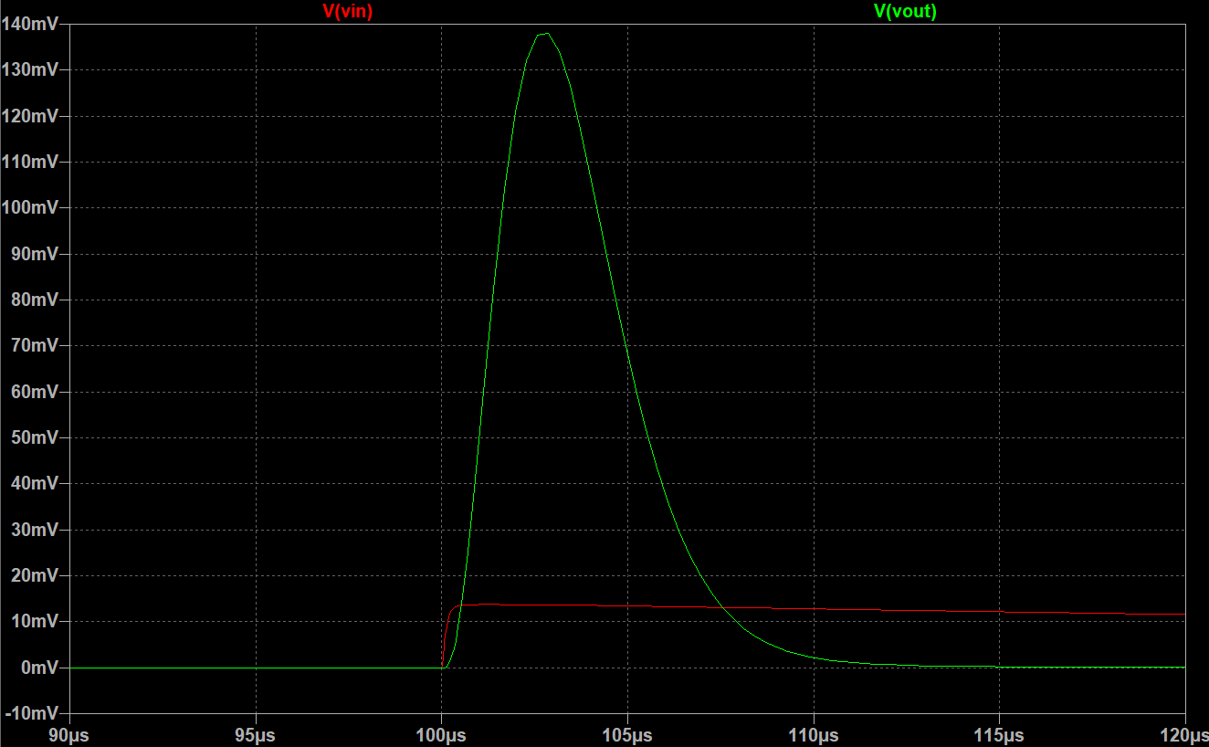
In the plots above, the value of FWHM has decreased to 3.8 μs, which is much closer to the ideal value of 3.6 μs and also consistent with the value advertised by Perevertaylo et al. (4 μs). If C3 is increased to 10 nF, the pulse from the preamplifier becomes much more rounded; voltage gain within the preamplifier increases dramatically but not linearly. Increase in C3 causes asymmetry of the shaped pulse to increase and also creates a greater range of time over which d
V/d
t along the leading edge of the pulse falls within the passband; these two effects produce an increase in FWHM. For this case (C3 = 10 nF), FWHM = 9.3 μs. I would guess that it’s possible to make the peak more symmetrical with a final stage of differentiation, but I haven’t explored this in any detail.
But enough with the simulator and onto construction!! The audiophile transistors that JEOL uses in its WDS preamplifiers are no longer manufactured, and so instead I’ll use the 2N4416 JFET for Q3 and the 2N5087 for Q4 (as I did in the simulation) in my replica. For Q5 and Q6, I’ll probably use the BC550C. For the detector coupling capacitor, I’d like to use no more than 1 nF – I need to contact Cremat and see why they used 10 nF. In order to reduce noise, I’ll probably lower the value of the feedback resistor to 50 MΩ and increase the value of the feedback capacitor to 2 pF, noting that tolerances at that capacitance are generally +/- 0.5 pF (i.e., 50% at 1 pF). I’ll replace transistors Q1 and Q2 with diodes and will keep resistor R3 in the circuit. I happen to have a couple LT1360 op amps on hand, and I’ll probably use one for the output buffer. I’ll probably end up building the shaping amplifier of Perevertaylo et al. with the LM6171 op amp (x 2). Those are just a few initial thoughts…


 Welcome to the Probe Software forum area!