OK, then are you saying that the Cameca instrument performs an extra step of converting from mono-polar to bipolar pulses, that the JEOL electronics does not? And that is the reason for the thinner PHA peaks on the Cameca pulse processing electronics?
Sorry if I ask dumb questions, I am not familiar at all with these electronic details.
Those are not dumb questions, those are actually very valid questions, just a bit in this context inpatient like "a-cart-attached-before-the-horse". The answer is, unless someone would invite me to peek into Jeol Probe electronics (at least to detector electronics), it is hard to tell.
So if we open the case where the Shapping of pulse takes place we see this (My kind reminder: DEADLY high voltage is present on part of such board):
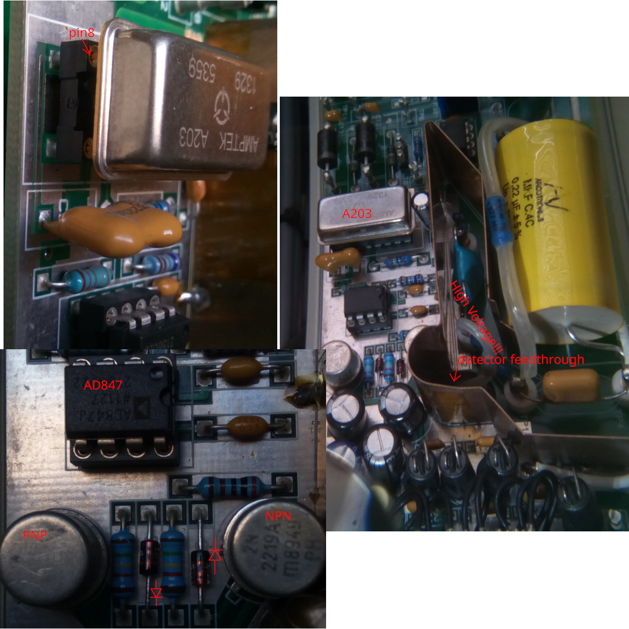
The Charge-Sensitive Preamplifier (CSP) and the Shapping Amplifier (SA) are packed inside single a single chip produced by Amptek - A203. The SA on that chip offers both: bipolar (pin9) and unipolar (pin8) outputs, however from visual inspection it is clear that Cameca uses unipolar (pin8, a clear trace from it, then around A203 to the capacitor for decoupling, which is required by documentation of A203) output from that chip and by components placed on the shielded ground plane (which points to very careful design for sensitive signal handling) it is clear that it does the 2nd differentiation on its own implementation (with OPAMP AD847). But why? I believe it is as A203 is not able to drive terminated (75ohm) coaxial cable on its own as A203 bipolar output is rated for 2kohm impedance - connecting such signal directly to terminated coaxial (75ohm) would lower down the amplitude a lot (x30 times), thus I think Cameca uses its own implementation with 2nd differentiation of monopolar pulses and (what I suspect from clearly visible two diodes and connection with NPN and PNP transistor pair) signal after that differentiation goes through class AB power amplifier (the short explanation what it is: https://www.elprocus.com/class-ab-amplifier/) as signal needs to be driven through few meter terminated coaxial cable to the gain and counting electronics. Just a side note: there are hardly any high speed OPAMPS which could directly drive such loads at these voltages (+/-15V), and thus the engineering of Cameca in this regard is a top notch.
So to answer the question if Jeol "shortcuts" on signal handling and thus PHA distribution suffers because of that - that would need similar inspection on Jeol hardware side: We need to know, what CPS and SA it uses (i.e. A203 is unique in its integration of both CSP and SA into single package - but it is possible to use separate CSP and SA chips (i.e. produced by Cremat inc.) to get the similar functionality), what kind of coaxial cable is used to send the signal from detector to counting board. Design for a few hundred of thousands of pulses a second is not complicated. However with Million pulses in second a single weak point in design can cause the amplitude drop.
This 75 ohm terminated coaxial cable is making me a headache for my planned experiment with external pulse generator. This means I will need to implement some fast class AB power amplifier if I want to simulate the pulses from the above presented circuit.
I however am skeptical if above described part of pipeline would produce observed differences in severity of PHA shift and broadness on Jeol probes. I introduced the description of bipolar pulse as a starting point to go further with explanation what happens next - when density of such pulses increase (count rate increase). We also can see the PHA shift on Cameca instruments and PHA distribution goes straight to hell when going to very high input count rates (like >1Mcps). And PHA shifting if using normal bias values is visible already from 20kcps and up.
So at first I want to present how I know the PHA shifts are produced on Cameca WDS hardware and in particular - how the bipolarity of pulses is causing that. Also my presented mitigation for "downsizing" (not to mistake with PHA shift) has a part in this story, and knowing if early shift can be mitigated by lowering the bias and increasing the gain can shed some light why Jeol PHA has more severe shifts (and broadening). I guess that there is not much difference of how Cameca converts unipolar to bipolar (doing math differentiation with OPAM), but how unipolar pulses looks like and differs by different handling of SA and CSP used by these two vendors. Unfortunately everything in pipeline before the bipolar pulse is more theoretical, as only bipolar output can be captured with oscilloscope. Nevertheless, knowing the process it is possible to reconstruct earlier shapes in the pipeline and find the possible reason even without opening the case and looking to the physical components of electronics.
I’ve attached datasheets for the Amptek A203 and also for the A250. From the photo on the A203 (and 206) datasheet, it appears that the can contains a mini-circuit board with relatively few (surface-mount) components; it is likely a very simple circuit, but the datasheet provides only minimal information on its design. Figure 8 from the datasheet for the presumably similar A250 provides a little more detail, but nothing is given on construction of the amplifier (still just an empty triangle).
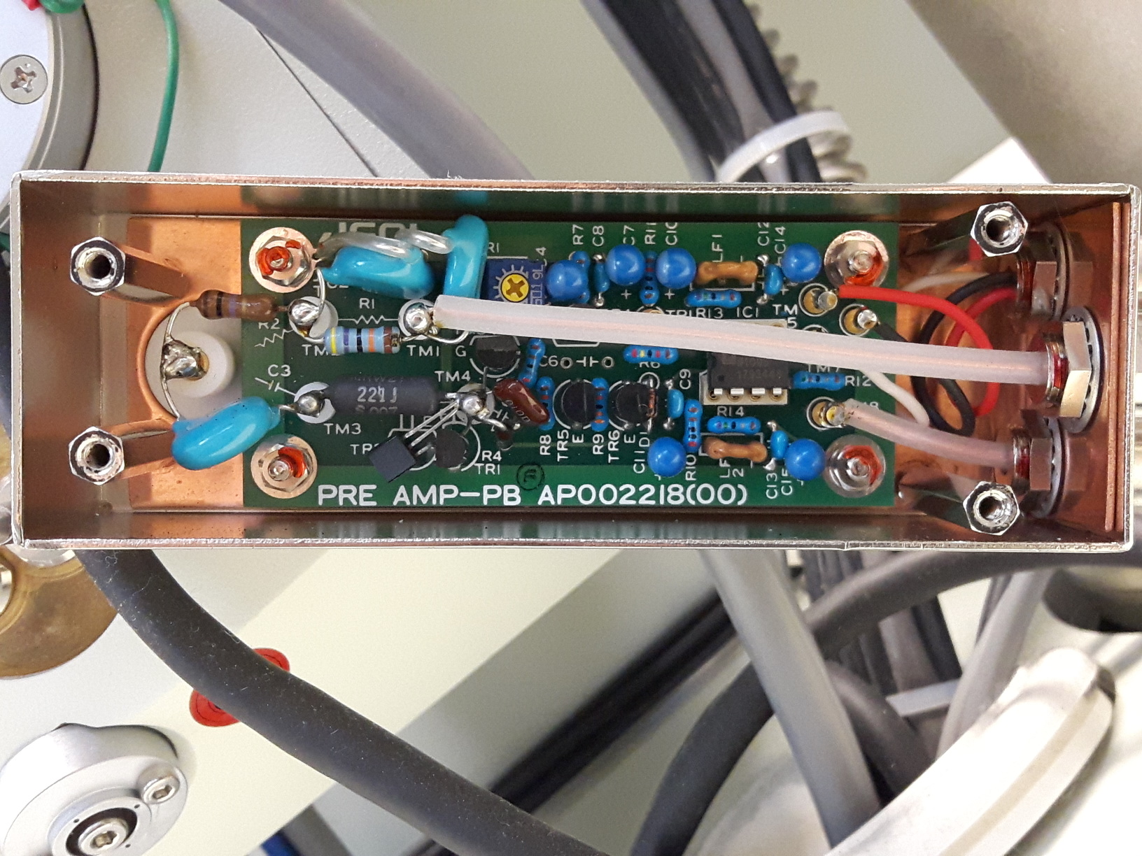
I don't understand the need for the push-pull transistors at the output of the CAMECA circuit, as the AD847 should be able to drive the cable directly.The JEOL WDS charge-sensitive preamplifier is constructed from discrete through-hole components (thank god); aside from capacitors, the component count is low. The transistors used in the circuit are of the low-noise type typically used in high quality audio amplifiers; I’ve attached datasheets. The circuit is shielded with copper plate and housed within a small steel box attached to the spectrometer. In the photo below, the long wire with thick insulation that runs parallel to the length of the box is the high voltage supply for the X-ray counter, with exposed high voltage at the binding posts (TM1, TM2) in the upper left along with two large, light blue ceramic bypass capacitors. The X-ray counter anode wire is in continuity with the heavily insulated terminal on the far left. The additional light blue ceramic capacitor on the far left is the coupling capacitor, C3, that blocks the X-ray counter anode bias; thus, aside from TM1 and TM2, the entire circuit board operates somewhere within the range +/-15 V. The red and white wires on the far-right are the respective +15 V and -15 V supplies, while the black wire is circuit common. The single test point (TP1) is mostly hidden by the insulated high voltage wire and is just barely visible adjacent to resistor R11; it is located at the noninverting input of the buffering op amp (see below). Variable resistor VR1 (see below) is located near the top margin of the board and has a yellow cross-slotted rotor within a square blue case. The six bulbous, blue components toward the right are 10 μF Ta bypass capacitors. A number of smaller, blue ceramic bypass capacitors are also visible, as are blue (metal film) color-coded resistors. Capacitor C5 (see below) is the glossy dark brown component immediately adjacent to the R8 label. The various transistors are all located in the lower middle of the circuit board and are housed in black plastic TO-92 cases. The circuit is designed to operate at low power.
I’ve constructed a simulation of the circuit in LTSpice (
free download!), with the schematic below generated from the software. I had to change transistors to ones that were available in the database, and I’ve noted each substitution on the schematic. My substitutes may serve reasonably well, but some resistor values likely need to be changed in order to bias the output more easily. Also, I substituted the AD811 op amp for the AD817; this should have no effect on behavior of the circuit as drawn below. For the sake of simplicity, I fed a 100 Hz sine function,
V(
t), into the input and arbitrarily assigned an amplitude of 1 mV (so
Vpeak-peak = 2 mV). With some fiddling of VR1, I was able to get the output centered at 0 V.
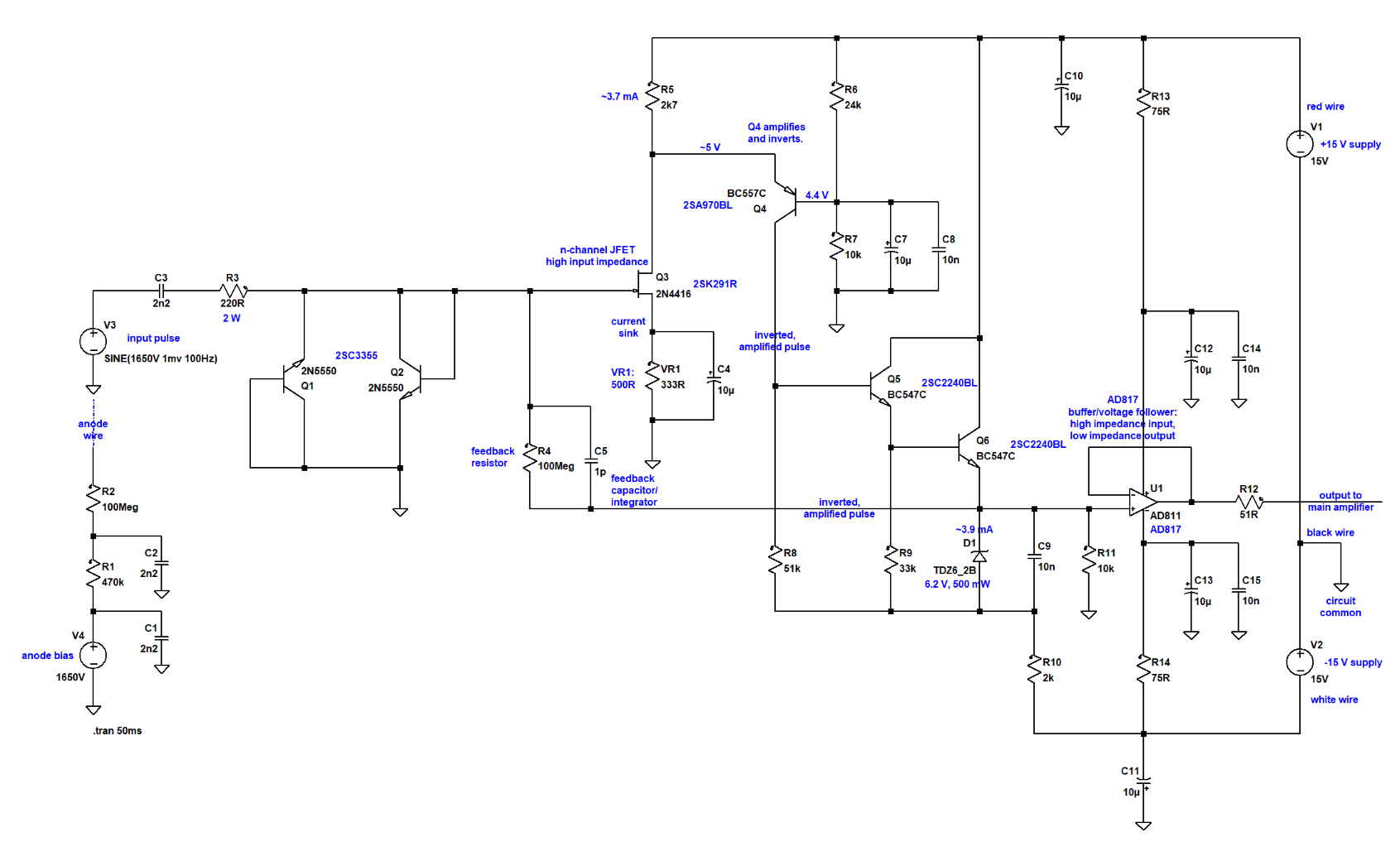
The circuit constitutes a charge-sensitive (and inverting) preamplifier. Variation in current at the input is inversely proportional to d
V/d
t at the output. Capacitor C3 is a coupling capacitor that blocks the bias (DC) on the X-ray counter anode
and also differentiates the “AC” pulse in conjunction with resistor R4. Resistor R3 and transistors Q1 and Q2 provide transient/reverse polarity protection; the two transistors normally do not conduct. Capacitor C5 (feedback capacitor, bridging the output and inverting input) is the characteristic feature of a charge-sensitive preamplifier and converts the pulse current to a voltage as it accumulates charge (integrates); note its tiny value (1 pF). Decay time of the pulse is given by R4 * C5 = 100 Mohm * 1 pF = 100 μs, producing a distinctively long pulse tail. Small signal gain of the circuit is referred to as "charge gain" and is given by 1/C5 = 1 V/pC. Resistor R4 also provides a path for DC (FET leakage) current and establishes a DC operating point for the amplifier. Amplification and inversion of the
differentiated input pulse is provided by PNP transistor Q4. The base of the transistor is biased at about 4.4 V using resistive divider R6-R7, and so the Q4 emitter (and Q3 drain) needs to be in the vicinity of 5.0 V for the transistor to remain in the “on” state continually (and conducting ~150 μA). The Q4 emitter voltage is set by varying variable resistor VR1 such that the current sink formed by it and JFET Q3 provides an appropriate voltage drop (around 10 V) across resistor R5; this requires that Q3 conduct about 3.7 mA between drain and source. Adjustment of VR1 also affects output DC bias. A critical feature of the JFET is that it has an extremely high input impedance, and, since only minimal leakage current flows through its gate, it does not contribute significant current to the pulse and thus provides a useful interface with the amplification circuit; the high input impedance is maintained by keeping the gate-drain voltage low (~5 V) and temperature < 25°C (and stable). Transistors Q5 and Q6 are arranged as a Darlington pair, and their purpose is to provide sufficient current (~3.9 mA) for operation of the 6.2 V/500 mW Zener diode, D1, used for biasing. They also provide a small amount of current (microamps) to the noninverting input of the AD817 buffering op amp.
The high-impedance signal output by the differentiation and amplification circuit cannot drive the low-impedance, high capacitance cable to the main amplifier, and so a high-speed op amp – in this case, the AD817 (datasheet attached) – is used as a buffer and cable driver. The op amp has an open-loop output impedance of 8 ohms, and so output impedance is set at 51 ohms by resistor R12. Guaranteed output current is 50 mA, though this is far greater than necessary. Further, the AD817 can drive an “unlimited” capacitive load (such as a length of cable) and has a guaranteed slew rate of 300 V/μs, unity gain bandwidth of 45 MHz, and 45 ns settling time to 0.1% (10 V step). Op amps of this nature are typically used in video applications and are characterized not only by high speed but also by low input voltage noise. Aside from being power-hungry, a general drawback of high-speed op amps is that the input bias current is enormous (3.3 microamps typical at 25°C for the AD817), and so input resistance is actually quite low – ~300 kohm in this case. Compared to others in its class, the op amp requires relatively little quiescent current (7.5 mA guaranteed compared to 6.3 mA for the AD847 and 18 mA for the AD811), and this ensures that relatively little heat is generated within the box. In its quiescent state, the AD817 dissipates no more than 225 mW. Transistor Q6 dissipates about 60 mW while conducting ~4 mA, and transistor Q3 dissipates about 15 mW while conducting a similar current. Transistors R5 and R10 dissipate ~40 mW and ~30 mW, respectively, and diode D1 dissipates about 25 mW. I would guess that air temperature inside the box is slightly higher than room temperature (by 1 or 2°C), but the circuit is always running and presumably at thermal equilibrium locally – obviously, it’s warmest near the op amp. In the vicinity of 25°C, the gate leakage current of JFET Q3 roughly doubles for every 10°C increase in temperature.
EDIT: Regarding the paragraph below, a sine function was not a good choice for use in the simulator. The small signal voltage gain of the circuit is inversely proportional to the capacitance of the feedback capacitor, C5. If the capacitance is doubled, the gain decreases roughly by a factor of two. For the JEOL circuit, the "charge gain" would be stated as 1/C5 = 1 V/pC. The total gain of the circuit depends as well on detector capacitance and the capacitance of C3 (2.2 nF). In the simulator, when feeding the input a 100 Hz sine function, V(t), with 1 mV amplitude, I see a small signal voltage gain of about 135 at the output relative to the input (see plot below). The phase is shifted by ~π/2 and is inverted relative to the input such that, if the input is a sine function, then the output is the negative cosine; this indicates that the output represents the negative of the first derivative (with respect to time) of the input (compare with figure 8.3 from Reed, 2nd ed., p. 93, below). The AC output voltage (in the absence of C5) is given by Vout = -C3 * R4 * dVin/dt = -0.22 s * dVin/dt; i.e., the AC output voltage depends on frequency of the sine function or on dV/dt at the leading edge of a pulse from the X-ray counter anode wire; the negative sign is due to inversion of the signal by transistor Q4 (PNP). Regarding the correction that I made to the figure from Reed, note that X-ray counter signal dV/dt initially is sharply negative, and so the signal is clearly inverted as well as differentiated to produce the output shown. Also, Reed's Figure 8.2 (not shown) is in error, as it is missing the feedback resistor required for
differentiation discharge of the feedback capacitor.
Figure 8.3 from Reed, “Electron Microprobe Analysis,” second edition:
EDIT: Reed’s two drawings show only the process of inversion and not differentiation. The tail on the amplified pulse is due to discharge of the feedback capacitor through the feedback resistor. This resistor is missing from Reed's Figure 8.2.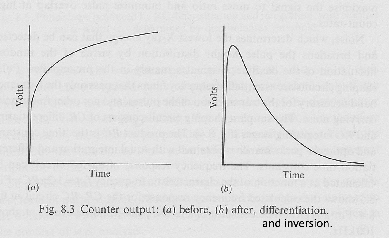
Simulator input and output:
EDIT: Ignore the plot below.
The following circuit (figure below) is equivalent functionally to the JEOL pre-amplifier, but, obviously, it is much simpler to interpret. Substitution of this circuit is made possible because the gain of the circuit is not set by the amplifier (constructed either from an op amp or from discrete components) but rather is set by external components
, as can be seen above in the expression for Vout. As above, if the input is a sine function, then the output is the negative cosine (and negative sine is present at the inverting input of the op amp). Disconnecting R4 produces cosine at the inverting input and negative sine at the output (with enormous gain). If R4 is reconnected and C5 disconnected, the output may oscillate.


 You cannot see "members only" boards if you are not a member, so please join the forum!