Author Topic: Spectral resolution and crystal size  (Read 27959 times)

John Donovan

  • Administrator
  • Emeritus
  • *****
  • Posts: 3275
  • Other duties as assigned...
    • Probe Software
Spectral resolution and crystal size
« on: July 16, 2013, 11:37:59 AM »
All,
Paul Carpenter and Gareth Seward and I have been discussing the effect of crystal size for JEOL and Cameca instruments and it is not entirely clear what effects this can have on spectral resolution.

Obviously, the Rowland Circle has a large effect on spectral resolution, JEOL = 140 mm (typically) and Cameca = 160 mm.  But assuming the same Rowland Circle what effect will the crystal size have on the spectral resolution?

Attached are some measurements I did a while back on Ti Ka in quartz and by luck I ran these scans all using the same scan width for each crystal type (PET/LPET and LIF/LLIF).  It would appear to my "eye-crometer" that the large area crystals have slightly better spectral resolution (narrower peaks) than the normal size crystals.

To me this makes no sense as the manufacturing of the large area crystals is more problematic and more subject to strain defects which should decrease the spectral resolution.

Please post any other peak scan data you have for your instrument (JEOL and Cameca) comparing Rowland Circle and crystal size effects on peak width (and also for that matter, peak shape).
« Last Edit: July 16, 2013, 11:44:18 AM by John Donovan »
John J. Donovan, Pres. 
(541) 343-3400

"Not Absolutely Certain, Yet Reliable"

John Donovan

  • Administrator
  • Emeritus
  • *****
  • Posts: 3275
  • Other duties as assigned...
    • Probe Software
Re: Spectral resolution and crystal size
« Reply #1 on: July 18, 2013, 10:39:10 AM »
Addendum: Now if you are referring to the low level background artifacts often seen on the large area crystals, you would be correct.  See attached below.

But I'm still not sure that explains why the FWHM appears to be better for the large area crystals.
John J. Donovan, Pres. 
(541) 343-3400

"Not Absolutely Certain, Yet Reliable"

John Donovan

  • Administrator
  • Emeritus
  • *****
  • Posts: 3275
  • Other duties as assigned...
    • Probe Software
Re: Spectral resolution and crystal size
« Reply #2 on: July 18, 2013, 10:47:03 AM »
Then again, by comparing the background artifacts of normal and large area crystals, I would probably pick very similar off-peak positions for both crystals. See attached.
John J. Donovan, Pres. 
(541) 343-3400

"Not Absolutely Certain, Yet Reliable"

Gseward

  • Global Moderator
  • Professor
  • *****
  • Posts: 134
Re: Spectral resolution and crystal size
« Reply #3 on: January 03, 2014, 11:38:59 AM »
John,

For comparison of 'artifacts' here is an example of PET/LPET wavescans of Ti ka on my SX100. CPS/nA, Log and linear intensity plot. Sorry if the images are not very good, I was in a rush!
 
Sp1 is LPET with Low Pressure detector
SP2 is PET with LP detector
SP5 is LPET with HP detector


I have been told that artifacts in the larger crystals are thought to be the result of 'misaligned sub-domains' in the surface of the diffracting crystal; these defects are unintentionally introduced during the forming/shaping process. The artifacts I see are similar to those in your scans, but as one might expect (given the proposed origin of the artifacts) differ slightly for individual LPET crystals.

Gareth

Gseward

  • Global Moderator
  • Professor
  • *****
  • Posts: 134
Re: Spectral resolution and crystal size
« Reply #4 on: January 03, 2014, 03:36:01 PM »
Here is a LTAP vs TAP comparison that I did during testing, when I first received my SX100. Si ka on Si metal. Al ka on Al metal. As John suggests, there is little difference in FWHM resolution (not visible in this plot). Note that the 2 LTAP xtals (light/dark blue, sp4 and sp1) show different artifacts: as well as the peak 'shoulders', seemingly-typical of L-type crystals, Sp1 also has distinct artifact-peaks on both sides of the ka peak.

Allow me to speculate, wildly: I wonder if the two types of artifact are the result of different 'defects' in the analyser crystal? Perhaps 'shoulders' are the result of distributed dislocations/plastic strain, where there is a continuum of rotation of the crystal lattice away from the desired (curved) orientation. Whereas the distinct artifact-peaks are the result of discrete domains/subgrains. This would be analogous to diffraction from a deformed vs recovered subgrained single crystal. I assume some plastic deformation is required to achieve the 2R curvature; perhaps this is incorrect?
However, should one expect more deformation in a larger crystal bent to the same radius?
Then again, perhaps the 'shoulders' are reflection phenomena?


Probeman

  • Emeritus
  • *****
  • Posts: 2836
  • Never sleeps...
    • John Donovan
Re: Spectral resolution and crystal size
« Reply #5 on: May 25, 2016, 01:34:23 PM »
I'm curious if anyone knows what causes the oddly shaped tails on the peaks with the LPET crystals but not the PET crystals:

http://probesoftware.com/smf/index.php?topic=18.msg57#msg57

Is it a manufacturing issue?
john
The only stupid question is the one not asked!

Probeman

  • Emeritus
  • *****
  • Posts: 2836
  • Never sleeps...
    • John Donovan
Re: Spectral resolution and crystal size
« Reply #6 on: October 10, 2017, 12:28:39 PM »
Hi Owen,
I ran a wavescan on my SiO2 standard using 2 TAP and 1 LTAP and I get smooth peaks.


I suspect that your large TAP is cracked!   If so, that hurts!  They aren't cheap xtals.
john
« Last Edit: April 14, 2020, 11:42:53 AM by John Donovan »
The only stupid question is the one not asked!

JohnF

  • Professor
  • ****
  • Posts: 105
  • CQ DX DE WA3BTA
    • John's EPMA
Re: Spectral resolution and crystal size
« Reply #7 on: November 26, 2017, 11:01:03 AM »
Aurelien and I too are concerned as we see some funky peak shapes on these (all? some? we need to do some systematic scans and report) large area mothers.  But, one huge  ;D question, is, are all of these coming from the same manufacturer? I thought, in the "old days" that they all(??) came from Ovonics. Also we know that in France that St Gobain makes this multilayers, so maybe Cameca's now?? come from there but in the past they came from Ovionics? Where does Jeol get theirs?? Do they see the same behavior?

Probeman

  • Emeritus
  • *****
  • Posts: 2836
  • Never sleeps...
    • John Donovan
Re: Spectral resolution and crystal size
« Reply #8 on: November 26, 2017, 11:55:31 AM »
Aurelien and I too are concerned as we see some funky peak shapes on these (all? some? we need to do some systematic scans and report) large area mothers.  But, one huge  ;D question, is, are all of these coming from the same manufacturer? I thought, in the "old days" that they all(??) came from Ovonics. Also we know that in France that St Gobain makes this multilayers, so maybe Cameca's now?? come from there but in the past they came from Ovionics? Where does Jeol get theirs?? Do they see the same behavior?

I think the correlation is the TAP nature of these wavescans.  One of the students in my EPMA class did a project on this unidentified peak in TiO2 (and Ti):

http://probesoftware.com/smf/index.php?topic=4.msg6427#msg6427

and I will post something tomorrow that I think is related, but in the meantime I think that the issue we're seeing is mostly with (large) TAP crystals (LTAP), but could also be a problem for very old normal size TAP crystals.

John Armstrong reported a while back that JEOL H type (small focal circle) TAP crystals, which are highly curved, show similar artifacts.  Here are some observations by Brian Joy and others on artifacts on JEOL crystals, both TAP and PET:

http://probesoftware.com/smf/index.php?topic=854.0

These crystals just tend to crack over time, and I would suggest that these cracks can produce these subtle (and not so subtle) peak shape changes.
john
The only stupid question is the one not asked!

Probeman

  • Emeritus
  • *****
  • Posts: 2836
  • Never sleeps...
    • John Donovan
Re: Spectral resolution and crystal size
« Reply #9 on: November 26, 2017, 11:58:34 AM »
OK, I found the comment by John Armstrong on H-type TAP crystals:

http://probesoftware.com/smf/index.php?topic=611.msg4215#msg4215

john
The only stupid question is the one not asked!

Probeman

  • Emeritus
  • *****
  • Posts: 2836
  • Never sleeps...
    • John Donovan
Re: Spectral resolution and crystal size
« Reply #10 on: December 04, 2017, 04:42:44 PM »
If there's a prize for worst Bragg crystal, I think our lab just won!

I don't normally use the PET crystal on our spectrometer 1 as it's a 4 crystal (PC1, PC2, TAP and PET), and usually we're just using the TAP or PC1 crystals.  But today we are analyzing Ti on all 5 spectrometers, and using MAN background for best sensitivity (I'll post the statistics on the SiO2 blank when it done), so we had to have PET on all 5 spectrometers.

Anyway, this morning I was tuning things up and noticed that the peak shape on spectrometer 1 was just not looking right as seen here:


The count rate was also 10 times less than what the other PET crystals were reporting. So I ran a wavescan on TiO2 and, just for reference, this is on spectrometer 4 (also PET), and is what one expects from ones EPMA:


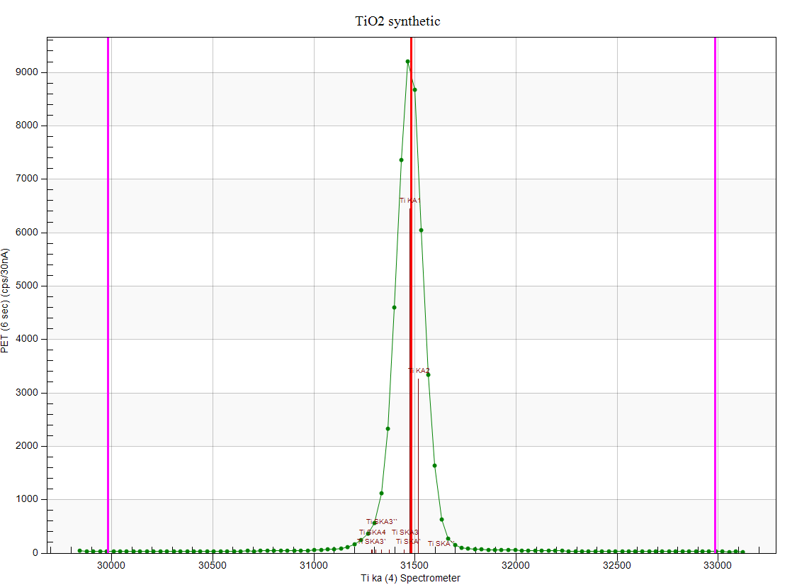
But for spectrometer 1, this is what we got:


I know, we all just threw up a little.  :'(

Looking back at some previous student runs, it appears that this change in peak shape occurred in some time in 2016, but I didn't see it until now.  I guess that is what happens when I'm only in the lab a few days a week...

We were planning on replacing the beam current regulator on Wednesday, so while we have the instrument vented, we're going to pop the cover off of spectrometer 1 and take a look at the crystal.  It's got to be the crystal because I also ran a scan on Mg on TAP on spectrometers 1 and 2, and they both look fine.

Jeez... well it's always something, isn't it?
john
« Last Edit: April 13, 2020, 10:22:23 PM by John Donovan »
The only stupid question is the one not asked!

Probeman

  • Emeritus
  • *****
  • Posts: 2836
  • Never sleeps...
    • John Donovan
Re: Spectral resolution and crystal size
« Reply #11 on: March 26, 2018, 05:02:53 PM »
So last week our instrument engineer replaced the cracked PET crystal in our SX100 with a good crystal from the SX50 which we just decommissioned and we pumped down and I did a scan on pure Ti and lo and behold the peak shape is beautiful again:


See the previous post above for the peak shape on the old crystal...

Now for the interesting part:  normally one would have to align the crystal by replacing the column separation windows in the instrument with Mylar windows and pump down the column leaving the spectrometers themselves up to air so one can reach in and adjust the crystal alignment while observing the x-ray count rate using a high order reflection of Fe Ka.

But our instrument engineer had a good idea: why not mount a laser pointer in the column separation window aperture and aim it at the center of the crystal, and adjust the crystal alignment until the laser dot shows up in the center of the detector window.  And you what, he did that, and as you can see from the above plot, it worked!

Yes, it's not quite within the Cameca recommendation of +/- 100 spectro units, but it's close (+178), which is similar to the other spectrometers!


And the count rate is quite comparable to the other similar sized PET crystals.

Edit: our engineer Steve says he thinks he can do better by having the shop machine an adapter ring for the laser pointer, as the above alignment was done using modeling clay to hold the pointer!
« Last Edit: April 13, 2020, 10:07:54 PM by John Donovan »
The only stupid question is the one not asked!

wrigke

  • Professor
  • ****
  • Posts: 40
Re: Spectral resolution and crystal size
« Reply #12 on: March 11, 2019, 03:18:29 PM »
My SX100R (shielded EPMA) was built around 2009.  I have the boxes in which the crystals shipped.  All of my crystals, layered and non-layered came from St Gobain, France.

I would like to have the opportunity to try new crystals with different geometries (e.g. Johann vs. Johannson) but would need to find a vendor who will make crystals on demand.  I think St. Gobain only sells through Cameca, not directly to the customer.

It would be nice to have some crystal manufacturers that could make high quality crystals on demand.

Karen Wright
« Last Edit: March 13, 2019, 07:41:41 AM by wrigke »

Probeman

  • Emeritus
  • *****
  • Posts: 2836
  • Never sleeps...
    • John Donovan
Re: Spectral resolution and crystal size
« Reply #13 on: March 11, 2019, 04:57:18 PM »
My SX100R (shielded EPMA) was built around 2009.  I have the boxes in which the crystals shipped.  All of my crystals, layered and non-layered came from St Gobain, France.

Incidentally, one of my colleagues attempted to have St Gobain make a custom crystal for their EPMA.  St Gobain was very reluctant to do so, and when they finally did it, it was very poorly done and ultimately unusable.

It would be nice to have some crystal manufacturers that could make high quality crystals on demand.

Karen Wright

Hi Karen,
Do you have any other details?  Was it a normal crystal or a multi-layer?

Are you asking if there are other sources for Bragg crystals?  Where does JEOL get their WDS crystals?  Also Thermo uses WDS crystals, do anyone know where they get them from?

I only know of the soft x-ray optics group at LBL.  When I was there I worked with Jim Underwood to develop better LDE crystals for quantifying N ka.

http://www.cxro.lbl.gov/

Jim's researchgate link is:

https://www.researchgate.net/scientific-contributions/2091855472_James_H_Underwood
john
« Last Edit: March 11, 2019, 10:07:47 PM by Probeman »
The only stupid question is the one not asked!

Philipp Poeml

  • Professor
  • ****
  • Posts: 219
Re: Spectral resolution and crystal size
« Reply #14 on: March 13, 2019, 01:50:14 AM »
Did you take into account that most likely most large crystals are Johansson and most "normal" crystals are Johann?

To me it seems much more difficult to align a Johansson crystal, because it is fully focussing, than a Johann crystal.

Anyway I wanted to ask about your alignment procedures, but maybe in another thread. There is something I do not yet fully understand. Because there are multi parameters you can adjust while aligning a crystal: Peak position and the position on the Rowland circle.